
One of the remarkable properties of diamond is its unsurpassed thermal conductivity, which is
five times higher than that of copper. As we all know, heat is conducted by electrons in metal, however, lattice vibrations are the key factor for the high thermal conductivity of diamond.
Due to the extraordinary high concentration of
atomic hydrogen produced by the very high temperatures of the arc discharging,
diamond films with high thermal conductivity can be easily obtained even at
relatively high growth rate by DC Arc Plasma Jet. The thermal conductivity of
our optical quality CVD diamond made by our company through DC Arc Plasma Jet approaches
that of the natural type IIa diamond, 2000W/mK. Thermal conductivity can be
tailored within the range of 800-2000 W/mK, and thus can be subdivided in to
different quality grades to meet the different needs of our customers in
different application fields. At present, CVD diamond made by our company is
used as mounts for high-power integrated circuits, laser diodes, GaN on Diamond
(GOD) and heat spreaders for satellite based electronic systems.
Specifications
Thermal Grade:
Thermal conductivity level:
Standard Medium: >1200W/m.k
High: >1500W/m.k
Excellent:>1800W/m.k (up to
2000W/m.k)
Flatness: <4um/cm
Density: 3.5g/cm3
Young's modulus: 1000-1100GPa
Growth side surface finish: <100 nm Ra
Nucleation side surface finish: <30 nm Ra
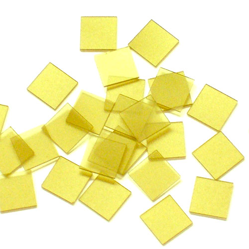
Standard Sizes
Double sides polished : Up to diameter 150 mm
As grown thickness: Between 0.3 mm and 1.5 mm
Polished thickness: Between 0.2 mm and 1.0 mm

86-311-83034449

sales@hediamond.cn

Copyright(c)Hebei Plasma Diamond Technology Co., Ltd. http://www.hediamond.cn/ Record number:冀ICP备07503481号-1
 冀公网安备13010402002676
 Qr code
 Online Service