

|
Presently, the efforts in R&D are focused in the following directions: 1.Introduction of new type microwave plasma CVD diamond reactors
|
|||||
|
(a)
|
|||||
|
(a) first homemade 75kW/915MHz ellipsoidal microwave plasma chemicalvapor deposition (MPCVD) reactor developed for growing large area high quality diamond film with high growth rate,
(b) 10kW/2.45 GHz TM01 mode circumferential antenna-ellipsoidal cavity type MPCVD reator,
(c) the plasma ignited in the reator |
|||||
|
High power microwave CVD diamond reactors with innovative design in the deposition chamber by which the coupling efficiency is enhanced, whilst the contamination to the microwave window is drastically reduced, have been successfully introduced, which include the ellipsoidal as well as the cylindrical type reactors.
|
|||||
|
2、Growth of large size high quality single crystal diamond
|
|||||
|
|
 |
|
|
||
|
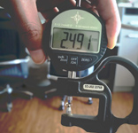
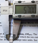
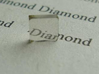
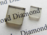
Large size (with a thickness exceeding 2mm) and high purity diamond single crystal grown by microwave plasma CVD. As per our examination, the sample color and clarity can all reach the gem grade level. With the optimization of process parameters, the crystal growth rate can reach up to 30 um/h, and the thickness tolerance of polishing sample can reach + / - 0.05 mm, crystallographic orientation deviation can reach ±2 ° and the surface roughness Ra < 30 nm. |
|||||
  |
|||||
|
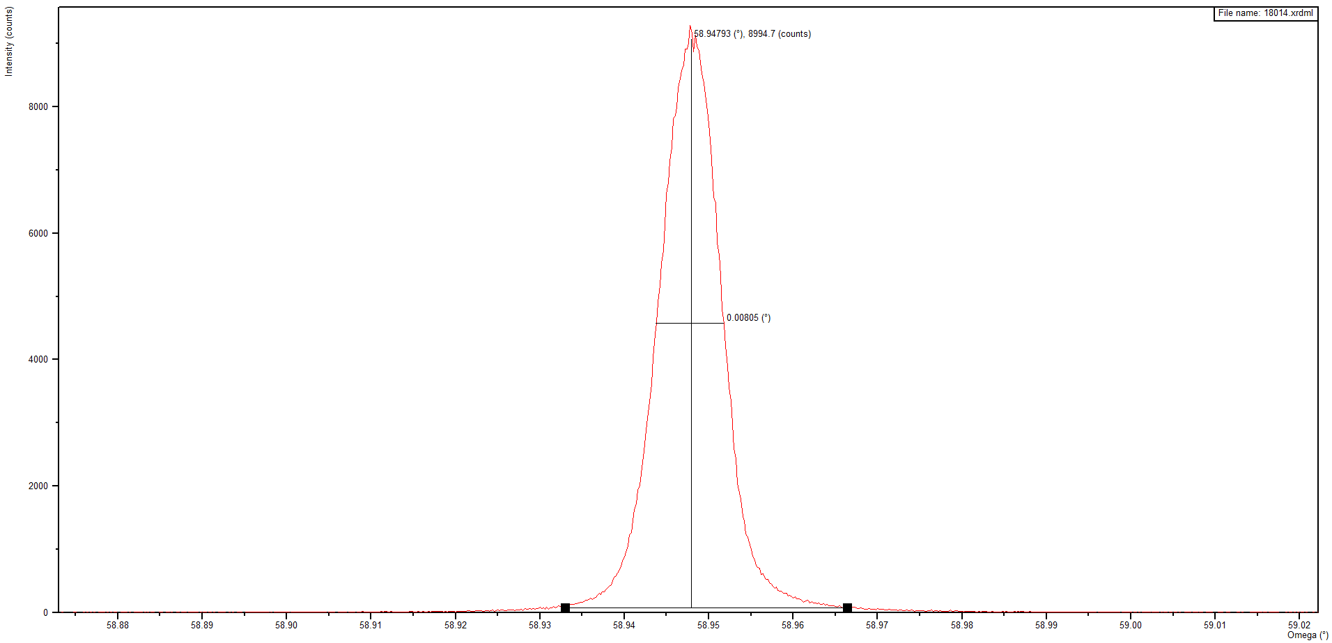
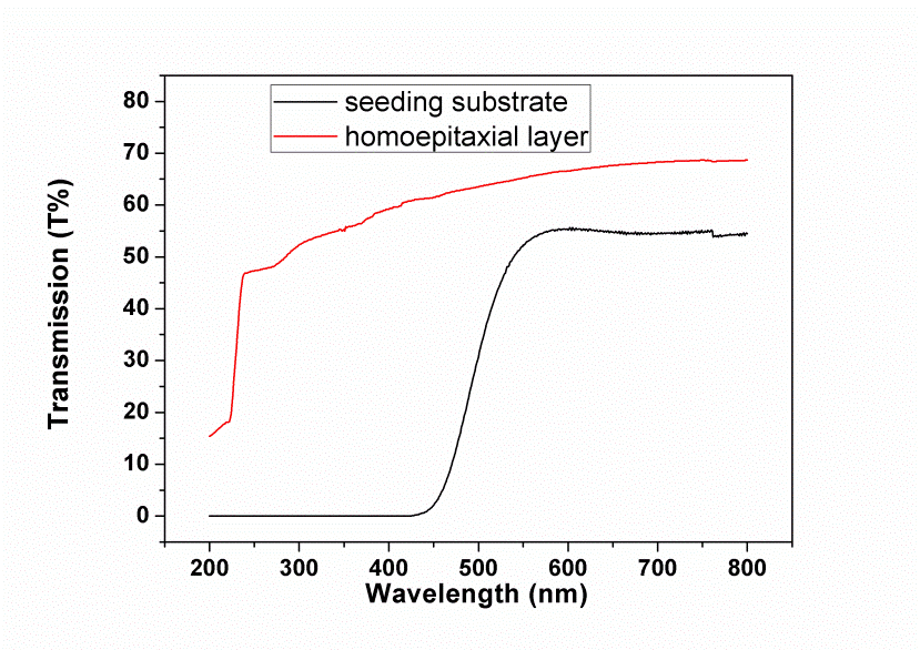
The full width at half maximum (FWHM) of diamond (400) peak in the X-ray rocking curve is only 0.008 (left), whilst the nitrogen content in the diamond single crystal isestimated to be less than 1.1 ppm from the tiny absorption peak at 270nm (right). Diamond single crystal with nitrogen content as low as 0.7ppm (700ppb) has also beensuccessfully obtained.
|
|||||
|
3. R&D for large area high quality freestanding diamond wafers suitable for high power laser window and high power microwave (Gyrotron) window, as well as for electronic applications. These microwave reactors are fully functional, and the process parameters for fabrication of large size, high quality freestanding diamond disks suitable for the use as optical,laser, and microwave windows have been optimized. |
|||||
|
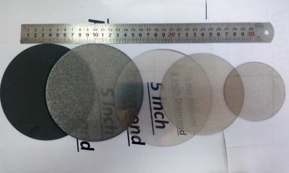
3-5 inch (φ76-127mm) crack-free and high quality diamond films were prepared by optimizing deposition parameters
|
|||||
|
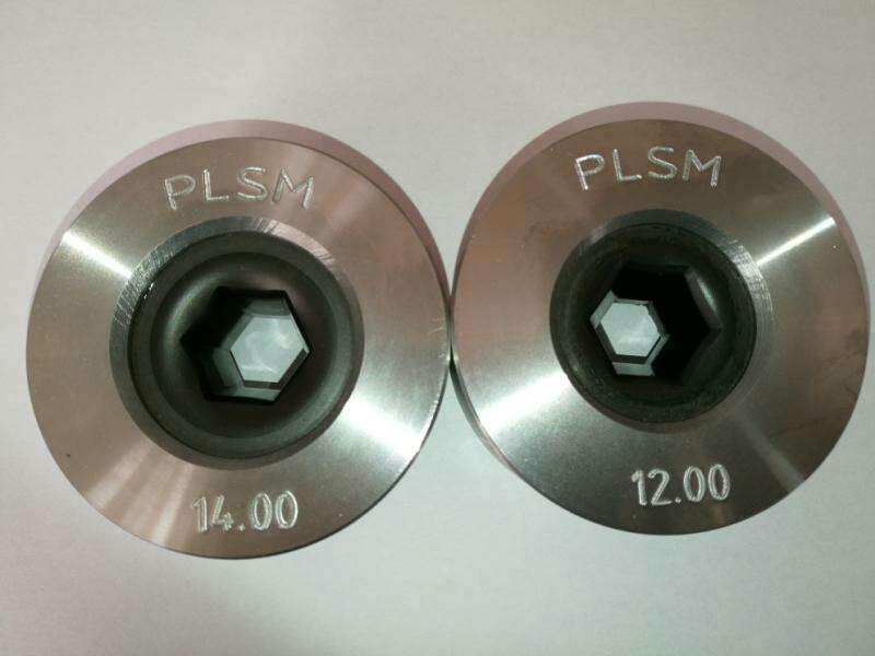
4. Thin film coatings by DC Arc Plasma Jet As compared to HFCVD and MWCVD, one of the advantages for daimond thin coatings on hard metal alloy substrate (cemented carbide) by DC arc Plasma Jet is that the higherdeposition rate may depress the outward diffusion of the cobalt, and is beneficial for promoting the adhesion of the diamond coatings on hard metal substrate. Taking the fulladvantages ofthe DC Arc Plasma Jet, we are successfully developed the technology for adherent dismond thin film coatings on hard metal tool components, as well as on SiCseals, and large size silicon wafers. Particularly, innovative technology for diamond thin film coatings on the inner surface of deep cavity molds and tools has developed, andpotentially can be used in a wide variety application fields. |
|||||
|
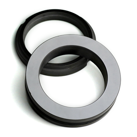
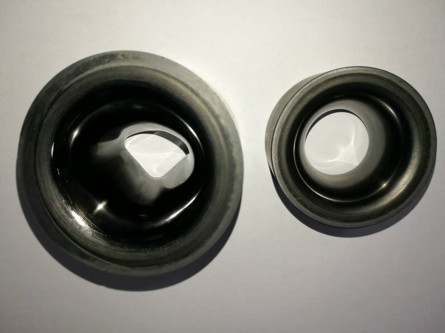
Diamond thin film coated SiC sealing rings (left) and wire drawing dieswith irregular deep cavity by DC Arc Plasma Jet |
|||||
|
5. Optimization for existing diamond film products Continuous efforts have been paying on the optimization for our existing diamond film products in according to the feedbacks of our customers all over the world, andparticularly, to the ever-growing demands in the new fields of innovative applications. We are sincerely welcome any proposals and suggestions, and particularly, any problemsin using our diamond film products. We are very happy to know, and are ready to cooperate for finding the solution as soon as possible. |
|||||

86-311-83034449

sales@hediamond.cn

No.46 Youyi south street,Qiaoxi District Shijiazhuang,050081,P.R.CHINA
Copyright(c)Hebei Plasma Diamond Technology Co., Ltd. http://www.hediamond.cn/ Record number:冀ICP备07503481号-1
 冀公网安备13010402002676
 Qr code
 (b)
(b)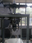 (c)
(c)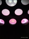
 Online Service